MoldERA
Preparation for Moldova's integration into the European Research Area and into the Community R&D Framework Programs on the basis of scientific excellence
Nano-roof reveals dislocations
01.02.2011Researchers in Moldova have fabricated nanometre-thin membranes of gallium nitride for the first time and investigated their nanostructure using electron microscopy. GaN is a large-bandgap semiconductor widely used in electronics applications such as high-temperature, high-power electronics and optoelectronics for light-emitting diodes and lasers. GaN is also biocompatible, piezoelectric and resistant to ionizing radiation, while the nanostructured material could be good for making spintronics devices.
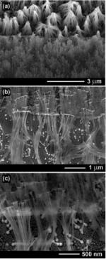
Dislocation networks, which form thanks to the mismatch between epitaxial layers and underlying substrates, are notoriously difficult to observe. They are a nuisance because they adversely affect the properties of electronic and optoelectronic materials and device structures. Ion Tiginyanu and colleagues have now developed a new technique that involves etching away high-quality crystalline material from bulk GaN epilayers to leave behind only the dislocation networks and a thin film to which the dislocations remain attached. The resulting nanostructures can then be imaged using scanning electron microscopy.
Tiginyanu's team used a modified version of the surface charge lithography (SCL) technique recently developed in their lab. SCL works by pre-treating a semiconductor surface using a low-energy ion beam to induce trapped negative charges that then effectively shield the material against subsequent photoelectrochemical (PEC) etching. For example, low-fluence Ar ions with energies as low as 0.4 keV can be applied to the GaN surface to do just this. The material remains transparent to ultraviolet light, however, so it can still be deeply etched.
GaN nano-roof
Because threading dislocations survive PEC etching, thanks to their negative charge, etching in potassium hydroxide can then create an ultrathin film membrane of GaN that resembles a "nano-roof" to which the dislocations are attached. "It is rather like pumping water from a lake covered by a layer of ice that has algae fixed on the surface – the network of algae can then clearly be seen," explained Tiginyanu.
According to the SEM images, each dislocation has a "root" shaped like a nanoball that has pronounced features such as clustering along definite lines and loops. "The dislocations are clustered about their roots and top ends forming mosaic structures," said Tiginyanu. The researchers also found that the dislocation networks emit mainly yellow light, while the GaN nano-roof emits both UV and yellow. The prevailing yellow part is probably related to point defects trapping the negative charge that shields the material against PEC etching.
Making nanometre-thin GaN membranes transparent to both electrons and UV-light is spectacular, says Tiginyanu. "Our preliminary investigations show that, in spite of their small thickness, the GaN nanomembranes have good electrical conductivity," he told nanotechweb.org. "Our technique for fabricating such thin gallium nitride membranes could help us better explore two-dimensional GaN-based structures predicted to be ferromagnetic with defect-induced half-metallic configurations, particularly important for spintronics applications."
The results were published in Materials Letters.
Source: www.nanotechweb.org


