MoldERA
Preparation for Moldova's integration into the European Research Area and into the Community R&D Framework Programs on the basis of scientific excellence


Surface writing produces designer nanostructures
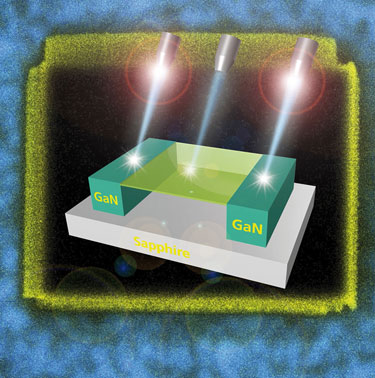
04.05.2012A new way to fabricate 3D nanostructures from gallium nitride using a focused ion beam (FIB) has been developed by researchers in Moldova, Australia, Germany and France. The technique, which involves directly writing a negative charge on the surface of GaN with the FIB and then photoelectrochemically etching the sample, allows ultrathin membranes and supporting nanocolumns to be fashioned in a controlled way. GaN is a large-bandgap semiconductor widely used in electronics applications such as high-temperature, high-power electronics and optoelectronics for light-emitting diodes and lasers. The material is also piezoelectric, so bridge-like GaN membranes might even find use in applications like nanoelectromechanical systems (NEMS).
Ion Tiginyanu and colleagues of the Moldova Academy of Sciences and Technical University of Moldova recently put forward a new way to make nanometre-thin membranes of gallium nitride hanging over a network of GaN threading-dislocation "whiskers" that act as a support. Their fabrication technique was based on etching away highly crystalline material from the GaN bulk epilayers, leaving behind only the negatively charged dislocation networks and a thin surface film to which the dislocations remain attached.
The team has now found that ultraviolet light can be used to etch away the whiskers themselves, leaving the ultrathin membrane hanging in free space without any support. To reproduce support structures, the researchers looked at subjecting selected areas of the top surface of the sample to a FIB treatment at relatively high fluences. "Our goal here was to introduce more lattice defects into the material making some of the FIB-treated top regions opaque to ultraviolet light," explains Tiginyanu.
High and low doses
To test their technique, the researchers subjected selected areas of a GaN sample to a focused beam of 30 keV Ga+ ions at a dose of around 1013 cm–2. They subjected the remaining surface regions to a gentler treatment with a lower fluence ion beam that induces trapped negative charges that then effectively shield the treated surface films against subsequent photoelectrochemical (PEC) etching. This part of the material remains transparent to ultraviolet light, however, so it can still be etched in depth.
As expected, the high-dose treated surface regions became opaque, so shielding the material underneath against subsequent photoelectrochemical treatment that produces nanostructures in form of nanowalls and columns. "These structures provide physical support for the ultrathin membranes above that emerge in the areas preliminarily subjected to the low-dose FIB treatment, " says Tiginyanu.
Different thicknesses possible
The researchers estimate that the thickness of the nanomembranes is about 15 nm, which is around the distance that the 30 keV Ga+ ion beam can penetrate the GaN matrix. "Such maskless fabrication of ultrathin GaN membranes suspended on GaN nanostructures is fascinating, and we can produce membranes with different thicknesses by controlling the energy of the FIB too, " he told nanotechweb.org.
The technique could be employed to make 3D nanostructures based on GaN and help make NEMS and photonic devices from this technologically important material, he added.
The work was reported in Physica Status Solidi – Rapid Research Letters.
Source: www.nanotechweb.rog
For the Romanian version of the news please access the news portal www.unimedia.md