MoldERA
Preparation for Moldova's integration into the European Research Area and into the Community R&D Framework Programs on the basis of scientific excellence


The International Society for Optics and Photonics (SPIE) highlights the development of “Ultra-thin membranes of non-layered crystalline solids” by our researchers Prof. Ion Tiginyanu and Dr. Veaceslav Popa
18.07.2011Ultra-thin solid membranes possess many unique properties not seen in their 3D counterparts. For example, graphene features very high breaking and tensile strengths,1 and is almost completely transparent to visible light.2 These and other properties render two-dimensional (2D) materials very useful for solar cell design,3 single-molecule detection,4 and many other applications. Synthetic constraints continue to pose a challenge.
Many researchers have focused their efforts on manufacturing ultra-thin solid membranes, including sheets of few-atomic layer graphene, boron nitride (BN), molybdenum disulfide (MoS2), bismuth telluride (Bi2Te3), bismuth selenide (Bi2Se3), and so on. Andre Geim and Konstantin Novoselov from the University of Manchester were awarded the 2010 Nobel Prize in Physics for the breakthrough of exploring graphene. To our knowledge, with the exception of our recent paper,5 all reported crystalline sheets are based on layered materials characterized by strongly anisotropic chemical bonding, where adjacent structural units are coupled by weak van der Waals interactions. It is these weak interactions that allow mechanical exfoliation of ultra-thin membranes.
Several years ago we proposed and developed a maskless lithography, surface charge lithography, for gallium nitride (GaN) micro- and nanostructuring. It is based on focused-ion-beam (FIB) direct writing of negative charge on the semiconductor surface, with subsequent photoelectrochemical (PEC) etching in potassium hydroxide (KOH) solution.6–8 The ion-beam-induced negative charge plays the role of shield against PEC etching, and therefore the combination of FIB treatment and PEC etching enables one to fabricate GaN nanostructures.
PEC dissolution is supported by holes provided by electron-hole pair generation under ultraviolet (UV) excitation. To dissolute the material in depth, i.e. under the top negatively-charged film, conditions for electrolyte penetration and efficient generation of electron-hole pairs should be provided. There is a simple way to achieve dissolution under the top shielding film, which involves electrolyte penetration from all sides and efficient generation of free carriers in depth due to high transparency of the top film to UV radiation. This can be achieved by using a low-energy (1keV or less) and a sufficiently low-dose ion treatment to avoid the formation of too many lattice defects contributing to the absorption increase. Figure 1 schematically illustrates the technological steps leading to the formation of a continuous thin membrane suspended over nanocolumns formed under the preliminarily-deposited top metal pads.

Figure 1. Fabrication of a suspended gallium nitride (GaN) membrane. KOH: Potassium hydroxide. PEC: Photoelectrochemical.
Our proposed method is also feasible for preparing large-area suspended ultra-thin nanoperforated membranes. The nanoholes within the membrane are responsible for membrane permeability to electrolyte species during dissolution. The transition from continuous to nanoperforated membranes is achieved by decreasing the dose of low-energy ion irradiation.
Regarding epitaxial GaN layers grown on sapphire substrates, it is not necessary to fabricate nanocolumns. Their role is readily played by whiskers representing threading dislocations, which survive during PEC etching due to their negative charge.5 Figure 2 shows scanning electron microscopy images of a GaN membrane hanging over networks of whiskers. To fabricate the membrane, an as-grown GaN epilayer was subjected to treatment by Ar+ (argon) ions, with the energy and dose as low as 0.4keV and 1011cm−2 respectively, followed by PEC etching in KOH solution under in-situ UV illumination.5 The thickness of the membrane is determined by the main projected range of the 0.4-keV Ar+ ions in the GaN matrix, which is 1.1nm.5
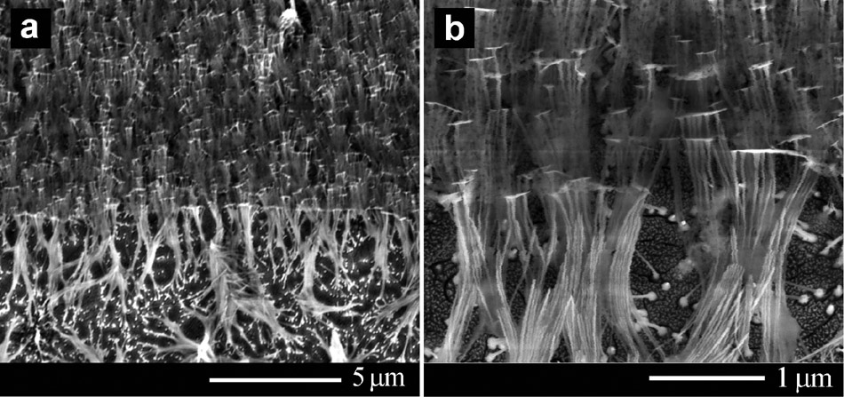
Figure 2. Scanning electron microscopy images of a GaN membrane hanging over whisker networks.
In spite of the few-atomic-layer thickness, the GaN membranes feature excellent mechanical stability. The ultra-thin GaN membranes are undulated, as demonstrated by atomic force microscopy (see Figure 3). Taking into account the piezoelectric characteristics of GaN, one can design specific devices based on ultra-thin membranes. Specifically, we are currently working on developing a peristaltic micro-pump based on a GaN membrane subjected to mechanical deformation by an applied alternating electric field (see Figure 4). The feasibility of such a device relies on nanomembrane elasticity and the intrinsic piezoelectric properties of GaN.

Figure 3. Atomic force microscopy image of a suspended GaN nanomembrane.

Figure 4. A peristaltic micro-pump based on a GaN nanomembrane.
In summary, we have fabricated 1nm-thick membranes of GaN. This achievement is very noteworthy, considering that this wide-band-gap (Eg=3.4eV at 300K) compound crystallizes in the hexagonal wurtzite structure with strong (partially ionic and covalent) bonds, i.e. it is not a layered material. Preliminary experiments show that the GaN ultra-thin membranes exhibit electrical conductivity. GaN biocompatibility opens unique opportunities for future research towards implementing nanomembranes in biomedicine (e.g. imaging), especially taking into account the intrinsic magnetic properties predicted for GaN sheets.9
More details at: www.spie.org