Site language:
MoldERA
Preparation for Moldova's integration into the European Research Area and into the Community R&D Framework Programs on the basis of scientific excellence


Physica Status Solidi
Physica Status Solidi
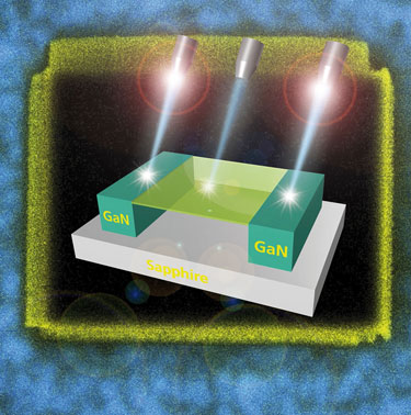
Surface writing produces designer nanostructures
Fri, 05/04/2012 - 07:40 — adminA new way to fabricate 3D nanostructures from gallium nitride using a focused ion beam (FIB) has been developed by researchers in Moldova, Australia, Germany and France. The technique, which involves directly writing a negative charge on the surface of GaN with the FIB and then photoelectrochemically etching the sample, allows ultrathin membranes and supporting nanocolumns to be fashioned in a controlled way. GaN is a large-bandgap semiconductor widely used in electronics applications such as high-temperature, high-power electronics and optoelectronics for light-emitting diodes and lasers.